
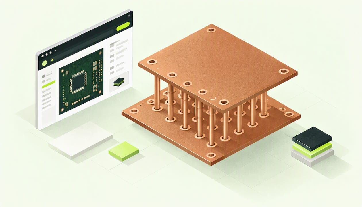
A good thermal via design comes down to four decisions: how many vias, how big, how far apart, and where they land. For a QFN-style exposed pad, a common starting point is a grid of 0.3 mm to 0.33 mm vias on a 1 mm to 1.25 mm pitch, connected straight into a copper plane that can actually shed the heat. The rest of this guide explains why those numbers work, where they stop helping, and what to check before you send the board to fab.
TL;DR
- Thermal vias are plated holes that carry heat vertically through the board. They only help if the heat has somewhere to go: a lower copper pad or plane, and ideally a heat sink or airflow.
- Start from the manufacturer's app note. One published guide suggests 0.3 mm to 0.33 mm diameter on a 1 mm to 1.25 mm pitch, and 11 to 22 vias for a 5 × 5 mm thermal pad.
- Returns diminish fast. Each extra via adds less than the one before, and a dense field raises solder voiding risk.
- Unfilled vias in an SMT pad wick solder. Use small holes, fill, or tenting, and agree the approach with your fabricator.
- Treat any calculation as an early estimate. Confirm with a measurement on a prototype.
Table of Contents
- What a thermal via actually does
- When thermal vias help, and when they don't
- The plane matters more than the via count
- Sizing and spacing: starting numbers
- A worked layout for a 5 × 5 mm pad
- Placement: close to the heat, tied into copper
- Manufacturing and assembly traps
- Our perspective
- Check the design and the parts in one place
- Other ways to move heat
- FAQ
- Sources
What a thermal via actually does
A thermal via is a plated through-hole between conductive layers, used to move heat from one layer to another rather than to carry current (Electronic Design). Typically it conducts heat from a component-side pad down through the stack to a cooler surface, such as a ground plane or a heat sink, using vertical conduction through the copper barrel (EDA Expert thermal guide).
FR-4 conducts heat poorly through its thickness. Copper conducts it well. A via is a small copper column that short-circuits the laminate. The effect is limited by what sits on both ends of the column: a pad that collects heat on top, and a plane or sink that spreads it out below.
When thermal vias help, and when they don't
They help most in conduction-cooled designs, where heat goes from the part into the PCB and then into a chassis, and in LED boards where all the heat has to cross the PCB to reach an external heat sink (Qpedia). Exposed-pad packages are the everyday case: vias placed within the pad move heat directly from the IC package into inner planes (Electronic Design).
They help less than people expect in other situations:
- No heat sink or airflow on the far side. Vias offer limited use if the air on the opposite side of the board is stagnant and nothing is attached there (EDA Expert). Another white paper reaches the same conclusion: without a heat sink, the cooling effect can be limited (Adam Research).
- Heat leaves through the top. For high-power BGAs where most heat goes up into a heat sink, vias have little effect on case temperature (Qpedia).
- Modest power. In six assembly layouts, calculated temperature differences with and without vias rarely exceeded 10%, and the gain grew with power dissipation (Adam Research).
The counterpoint is real too. A 2010 model of a 10 mm × 10 mm via array under a QFN-style part showed a 90% reduction in overall PCB thermal resistance against a no-via baseline (Qpedia). Both results are true because the board, the copper, and the cooling path differ. That is why you check your own case instead of copying a rule.
The plane matters more than the via count
A 2024 simulation published by the Printed Circuit Engineering Association found that an underlying plane lowered the heated-pad temperature by 28.5 °C, about 45%, while vias without a lower pad or plane had almost zero effect (PCEA). A companion article argues that thermal vias give only marginal benefit next to adding copper directly under the heated pad, and that they can be an inefficient use of board area (PCD&F).
The practical reading: do not ask "how many vias?" before you ask "where does the heat land?" Vias are a connector between two copper areas. If the bottom copper is a small island, the vias just move the bottleneck.
Sizing and spacing: starting numbers
The best-documented starting point comes from Diodes Incorporated's TQFN thermal pad application note (August 2019). It gives a general guideline of 1 mm to 1.25 mm via pitch and 0.3 mm to 0.33 mm diameter, and a recommended range of 11 to 22 vias for a 5 × 5 mm thermal pad (Diodes AN1151). The same note says that beyond roughly 22 to 55 vias, adding more does not significantly improve heat transfer and may complicate assembly by raising the risk of solder voiding.

Diameter and plating
Larger and more numerous vias generally improve heat dissipation, but a 2023 study also found that excessively thick copper plating can, in some cases, increase thermal resistance (MDPI Applied Sciences). Do not ask for heavier plating as a free thermal upgrade without checking your fabricator's capability and the study's conditions.
The diameter trade-off is also mechanical. Larger vias lower thermal resistance, but when they sit under an SMT package they invite solder wicking, so designers end up compromising between via size and quantity (Electronic Design).
Open versus filled
An open via conducts only through its plated wall. Cree's LED application note gives an example: a 0.6 mm open via with 35 µm plating has an effective area of 0.06 mm², against 0.28 mm² for a solid via (Cree). Filling the barrel with conductive material helps thermally, and it also solves wicking. It costs more, so decide per board.
Cree's own calculation shows how much the via count can matter on a small LED board: about 12 °C/W for a 270 mm² board with five 0.6 mm solid vias, versus about 30 °C/W without vias. Its simulations show results depend on via number, diameter and fill, board thickness, and copper pad size (Cree).
Diminishing returns
In the PCD&F simulations, each additional via contributed less than the previous one, and the marginal contribution declined exponentially (PCD&F). The Qpedia model likewise saw gains flatten after about an 80% improvement. Plan to fill the pad sensibly, then spend your effort on the plane and the cooling path.
Array pattern
In a 2023 test on a high-lead QFN package, square distributions outperformed circular ones when the via count was large, and 25 vias ran 1.8 °C cooler than 9 vias (MDPI Applied Sciences). That is a small gain in one package. Use it as a tiebreaker, not a design rule.
A worked layout for a 5 × 5 mm pad
This is an illustration built on the app-note numbers above, not a measured result. Say you have a QFN with a 5 × 5 mm exposed pad.
- Choose a 0.3 mm finished hole and a 1.0 mm to 1.25 mm pitch, per the Diodes guideline.
- A 4 × 4 grid at 1.2 mm pitch spans 3.6 mm in each direction, which sits inside the pad with margin and gives 16 vias, inside the 11 to 22 range.
- Make the pad on the opposite layer at least as large as the array, and connect it to a solid ground plane, not a thin trace.
- Connect the vias to the pad and planes with no thermal relief spokes.
- Decide on tenting or filling before releasing fab files.
Then check the result. Estimate power dissipation first (our power dissipation guide covers three formulas) and compare the predicted temperature rise against your part's limit.
Placement: close to the heat, tied into copper
For TQFN parts, put the vias in the PCB thermal landing so they carry heat to internal copper planes. On boards with more than eight layers, connect them to one or two ground planes closer to the component (MDPI Applied Sciences). The same research team stresses that vias must sit as close as possible to the heat source, directly beneath the thermal pad, because efficiency drops sharply when they are misplaced.
Two more placement rules:
- Size the pad to the package. For PQFN and QFN parts, NXP advises matching the center pad to the maximum dimension of the exposed heat spreader, which maximizes the number of possible vias and helps self-centering (NXP AN3778).
- No thermal reliefs. Thermal vias should connect directly to internal or external copper planes. Reliefs, useful for hand soldering, choke the heat path (Electronic Design).
Manufacturing and assembly traps
The thermal win is easy to lose on the assembly line.
Solder wicking. During reflow, solder can flow down an unfilled via, leaving less solder under the exposed pad and sometimes causing solder balling (Diodes AN1151). Holes of 0.3 mm or smaller, or via filling, reduce the problem (EDA Expert).
Tenting the back. Covering vias with solder mask on the underside can stop wicking, but it can trap corrosive flux residue unless you use a proper no-clean process (Electronic Design).
Solder voids. Too many vias may disturb the paste volume under the pad. Diodes provides pad-layout recommendations to reduce the risk. If your part's datasheet gives a land pattern, start there, and ask your assembler about stencil aperture windowing.
A short fab checklist: confirm minimum hole size and aspect ratio, whether via fill is offered and at what cost, and whether the fab can tent on one side only.

Our perspective
We see thermal vias mostly at the moment a prototype runs hotter than someone hoped. The pattern is familiar: the schematic was fine, the footprint came from a library, and nobody asked where the heat would go. Our view is that via design is the last of three steps, not the first.
First, estimate the watts. Second, work out the cooling path: copper area, plane, heat sink, enclosure. Third, size the vias to connect the first two. That order keeps you from putting 40 holes under a part that needed a bigger bottom pad.
It is also why we built a thermal map into the Circuit Designer: you enter watts, see how hot each part and the board will run in 3D, and see the source behind each value. It is an early estimate for comparing options, never a sign-off. A prototype with a thermocouple or thermal camera has the final say. Read our PCB thermal analysis guide for how to go from estimate to measurement.
— Matthew
Check the design and the parts in one place
If your board is in KiCad, Circuit Designer opens the project in your browser, with schematic, board, layer stackup and a priced BOM. The stackup view helps you see which plane your vias will actually land on. Design files stay in your browser unless you save them to your account. When a heat-driven change swaps a part, the BOM pricing tool re-prices the build at your quantity.
Other ways to move heat
Thermal vias are the least expensive thermal management method, but they are often insufficient alone and should be combined with copper planes, via fill, or heat sinks (EDA Expert). In practice:
| Approach | Good for | Watch out for |
|---|---|---|
| Thermal via array | Exposed-pad ICs, LED boards | Needs a lower pad or plane; wicking and voids |
| Larger copper pour or plane | Spreading heat sideways and downward | Board area, stackup cost |
| Filled vias | Higher conduction, no wicking | Extra fab cost |
| Heat sink or chassis contact | Moving heat out of the board | Mechanical design, cooling on the far side |
If the part dissipates a lot and the heat exits through the top, a heat sink on the package matters more than anything under it.
FAQ
How many thermal vias do I need?
There is no universal number. One manufacturer's note suggests 11 to 22 vias for a 5 × 5 mm thermal pad, and says returns fade beyond that. Start there, then check the result against your power and temperature limit.
What diameter should thermal vias be?
A general guideline is 0.3 mm to 0.33 mm on a 1 mm to 1.25 mm pitch. Holes of 0.3 mm or smaller also reduce solder wicking. Confirm what your fabricator can do reliably.
Should thermal vias be filled or tented?
Filled vias conduct better and stop wicking, but cost more. Tenting the back stops solder flowing through, though it can trap flux residue without a proper no-clean process. Choose based on power level, budget and your assembler's process.
Do thermal vias work without a heat sink?
Only to a limited degree. Research shows vias without a lower pad or plane did almost nothing in one simulation, and other work says stagnant air on the far side limits the benefit. Give the heat a copper plane at least, and a heat sink or airflow if power is significant.
Sources
- Motor-Driver PCB Layout Guidelines (Part 1), Electronic Design
- The Printed Circuit Designer's Guide to Thermal Management, EDA Expert
- Understanding and Optimizing Thermal Vias, Qpedia
- AN1151 TQFN Package Thermal Pad Via Design Guide, Diodes Incorporated
- Effect of Thermal via Design on Heat Dissipation, MDPI Applied Sciences
- Thermal Vias are Ineffective. Here's Why, PCD&F
- PCB Layout Guidelines for PQFN/QFN Style Packages, NXP AN3778
- Optimizing PCB Thermal Performance for Cree XLamp LEDs
- Optimizing PCB Thermal Performance for XLamp LEDs, Cree
- Brooks, Printed Circuit Engineering Association Magazine
- How effective are Thermal Vias?, Adam Research